(China (Mainland))


Product Summary
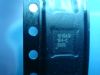
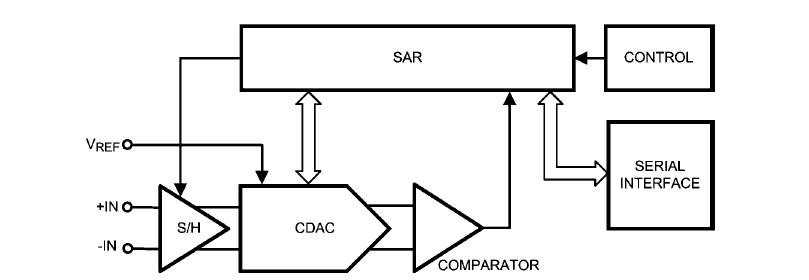
The ADC161S626CIMME/NOPB is a 16-bit successive-approximation register (SAR) Analog-to-Digital converter (ADC) with a maximum sampling rate of 250 kSPS. The ADC161S626CIMME/NOPB has a minimum signal span accuracy of ± 0.003% over the temperate range of -40℃ to +85℃. The converter features a differential analog input with an excellent common-mode signal rejection ratio of 85 dB, making the ADC161S626CIMME/NOPB suitable for noisy environments. The ADC161S626CIMME/NOPB operates with a single analog supply (VA) and a separate digital input/output (VIO) supply. VA can range from +4.5V to +5.5V and VIO can range from +2.7V to +5.5V. This allows a system designer to maximize performance and minimize power consumption by operating the analog portion of the ADC at a VA of +5V while interfacing with a +3.3V controller. The serial data output is binary 2’s complement and is SPI compatible. The performance of the ADC161S626CIMME/NOPB is guaranteed over temperature at clock rates of 1 MHz to 5 MHz and reference voltages of +2.5V to +5.5V. The ADC161S626CIMME/NOPB is available in a small 10-lead MSOP package. The high accuracy, differential input, low power consumption, and small size make the ADC161S626CIMME/NOPB ideal for direct connection to bridge sensors and transducers in battery operated systems or remote data acquisition applications.
Parametrics
ADC161S626CIMME/NOPB absolute maximum ratings: (1)Analog Supply Voltage VA: -0.3V to 6.5V; (2)Digital I/O Supply Voltage VIO: -0.3V to 6.5V; (3)Voltage on Any Analog Input Pin to GND: -0.3V to (VA + 0.3V); (4)Voltage on Any Digital Input Pin to GND: -0.3V to (VIO + 0.3V); (5)Input Current at Any Pin: ±10 mA; (6)Package Input Current: ±50 mA; (7)ESD Susceptibility: Human Body Model 2500V, Machine Model 250V, Charge Device Model 1250V; (8)Junction Temperature: +150℃; (9)Storage Temperature: -65℃ to +150℃.
Features
ADC161S626CIMME/NOPB features: (1)16-bit resolution with no missing codes; (2)Guaranteed performance from 50 to 250 kSPS; (3)±0.003% signal span accuracy; (4)Separate Digital Input/Output Supply; (5)True differential input; (6)External voltage reference range of +0.5V to VA; (7)Zero-Power Track Mode with 0 μsec wake-up delay; (8)Wide input common-mode voltage range of 0V to VA; (9)SPI/QSPI/MICROWIRE compatible Serial Interface; (10)Operating temperature range of -40℃ to +85℃; (11)Small MSOP-10 package.
Diagrams
| Image | Part No | Mfg | Description |  |
Pricing (USD) |
Quantity | ||||||||||||
|---|---|---|---|---|---|---|---|---|---|---|---|---|---|---|---|---|---|---|
 |
 ADC161S626CIMME/NOPB |
National Semiconductor (TI) |
ADC (A/D Converters) |
Data Sheet |
|
|
||||||||||||
| Image | Part No | Mfg | Description | |
Pricing (USD) |
Quantity | ||||||||||||
 |
ADC1001 |
Other |
|
Data Sheet |
Negotiable |
|
||||||||||||
 |
ADC1001CCJ |
|
IC ADC 10BIT MPU COMPAT 20-CDIP |
Data Sheet |
Negotiable |
|
||||||||||||
|
ADC1001CCJ-1 |
|
IC ADC 10BIT MPU COMPAT 20-CDIP |
Data Sheet |
Negotiable |
|
||||||||||||
 |
ADC1002S020HL/C1,1 |
NXP Semiconductors |
ADC (A/D Converters) SGL 10BIT ADC 20MSPS |
Data Sheet |
|
|
||||||||||||
|
ADC1002S020HL/C1:1 |
NXP Semiconductors |
ADC (A/D Converters) ADC Single 20MSPS 10bit Parallel 32pin |
Data Sheet |
|
|
||||||||||||
|
ADC10030 |
Other |
|
Data Sheet |
Negotiable |
|
||||||||||||