(China (Mainland))

Product Summary
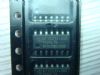
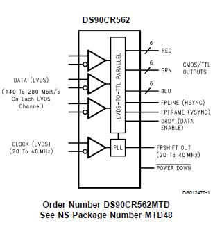
The DS90CR562MTD is a receiver which converts the LVDS data streams back into 21 bits of CMOS/TTL data. At a transmit clock frequency of 40 MHz, 18 bits of RGB data and 3 bits of LCD timing and control data (FPLINE, FPFRAME, DRDY) are transmitted at a rate of 280 Mbps per LVDS data channel. Using a 40 MHz clock, the data throughput is 105 Megabytes per second. The DS90CR562MTD is offered with rising edge data strobes for convenient interface with a variety of graphics and LCD panel controllers. This chipset is an ideal means to solve EMI and cable size problems associated with wide, high speed TTL interfaces.
Parametrics
DS90CR562MTD absolute maximum ratings: (1)Supply Voltage (VCC): -0.3V to +6V; (2)CMOS/TTL Input Voltage: -0.3V to (VCC + 0.3V); (3)CMOS/TTL Ouput Voltage: -0.3V to (VCC + 0.3V); (4)LVDS Receiver Input Voltage: -0.3V to (VCC + 0.3V); (5)LVDS Receiver Input Voltage: -0.3V to (VCC + 0.3V); (6)LVDS Output Short Circuit Duration: continuous; (7)Junction Temperature: +150℃; (8)Storage Temperature Range: -65℃ to +150℃; (9)Lead Temperature (Soldering, 4 sec.): +260℃; (10)Maximum Power Dissipation @ +25℃ MTD48 (TSSOP) Package: 1.89W; (11)Package Derating: 15 mW/℃ above +25℃.
Features
DS90CR562MTD features: (1)Up to 105 Megabyte/sec bandwidth; (2)Narrow bus reduces cable size and cost; (3)290 mV swing LVDS devices for low EMI; (4)Low power CMOS design; (5)Power-down mode; (6)PLL requires no external components; (7)Low profile 48-lead TSSOP package; (8)Rising edge data strobe; (9)Compatible with TIA/EIA-644 LVDS standard.
Diagrams
| Image | Part No | Mfg | Description |  |
Pricing (USD) |
Quantity | ||||
|---|---|---|---|---|---|---|---|---|---|---|
 |
 DS90CR562MTD |
|
IC RCVR LVDS FPD 18BIT 48-TSSOP |
Data Sheet |
Negotiable |
|
||||
|
DS90CR562MTDX |
|
IC RCVR LVDS FPD 18BIT 48-TSSOP |
Data Sheet |
Negotiable |
|
||||