(China (Mainland))

Product Summary
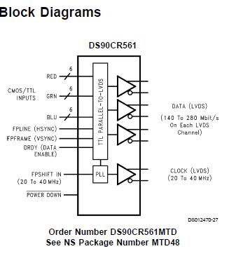
The DS90CR561MTD is a transmitter which converts 21 bits of CMOS/TTL data into three LVDS (Low Voltage Differential Signaling) data streams. A phase-locked transmit clock is transmitted in parallel with the data streams over a fourth LVDS link. Every cycle of the transmit clock 21 bits of input data are sampled and transmitted. The DS90CR561MTD is offered with rising edge data strobes for convenient interface with a variety of graphics and LCD panel controllers. This chipset is an ideal means to solve EMI and cable size problems associated with wide, high speed TTL interfaces.
Parametrics
DS90CR561MTD absoute maximum ratings: (1)Supply Voltage (VCC): -0.3V to +6V; (2)CMOS/TTL Input Voltage: -0.3V to (VCC + 0.3V); (3)CMOS/TTL Ouput Voltage: -0.3V to (VCC + 0.3V); (4)LVDS Receiver Input Voltage: -0.3V to (VCC + 0.3V); (5)LVDS Receiver Input Voltage: -0.3V to (VCC + 0.3V); (6)LVDS Output Short Circuit Duration: continuous; (7)Junction Temperature: +150℃; (8)Storage Temperature Range: -65℃ to +150℃; (9)Lead Temperature (Soldering, 4 sec.): +260℃; (10)Maximum Power Dissipation @ +25℃ MTD48 (TSSOP) Package: 1.98W; (11)Package Derating: 16 mW/℃ above +25℃.
Features
DS90CR561MTD features: (1)Up to 105 Megabyte/sec bandwidth; (2)Narrow bus reduces cable size and cost; (3)290 mV swing LVDS devices for low EMI; (4)Low power CMOS design; (5)Power-down mode; (6)PLL requires no external components; (7)Low profile 48-lead TSSOP package; (8)Rising edge data strobe; (9)Compatible with TIA/EIA-644 LVDS standard.
Diagrams
| Image | Part No | Mfg | Description |  |
Pricing (USD) |
Quantity | ||||
|---|---|---|---|---|---|---|---|---|---|---|
 |
 DS90CR561MTD |
|
IC TX LVDS FPD 18BIT 48-TSSOP |
Data Sheet |
Negotiable |
|
||||
|
DS90CR561MTDX |
|
IC TX LVDS COLOR FPD LNK 48TSSOP |
Data Sheet |
Negotiable |
|
||||